
Sapphire Dielectric Constant: RF Substrate Guide
Sapphire Dielectric Constant: A B2B Procurement Guide for RF and High-Power Electronics
Featured Snippet (≤50 words): The dielectric constant of single-crystal sapphire is ε_r∥ = 11.6 parallel to the c-axis and ε_r⊥ = 9.4 perpendicular to the c-axis (NIST SRD 150, 1 MHz reference). With loss tangent 3×10⁻⁵ to 8.6×10⁻⁵ across 10 Hz to 3 GHz and dielectric strength up to 48 kV/mm, sapphire is the substrate of choice for high-Q resonators, 5G RF filters, and quantum devices.
Introduction
Single-crystal sapphire (synthetic α-Al₂O₃) is the substrate of choice for high-performance RF, microwave, and millimeter-wave applications due to its ultra-low loss tangent (3×10⁻⁵ to 8.6×10⁻⁵ across 10 Hz to 3 GHz) and stable dielectric properties across wide temperature and frequency ranges. Unlike polycrystalline alumina or fused silica, sapphire exhibits a well-characterized anisotropic dielectric constant (ε_r∥ = 11.6 parallel to the c-axis, ε_r⊥ = 9.4 perpendicular to the c-axis) that enables precision impedance matching in high-Q resonators, narrowband filters, and superconducting quantum devices.
This guide provides NIST-validated dielectric constants, frequency- and temperature-dependence data, and a material comparison matrix to help RF engineers, microwave designers, and B2B procurement teams select the optimal sapphire grade for their application. The data is sourced from NIST Standard Reference Database 150, IEEE Transactions on Microwave Theory and Techniques, peer-reviewed journal articles (Optica Applied Optics, SPIE Proceedings), and HEM-grown single-crystal sapphire supplier datasheets.
Test methods used in this guide (see Section 7 for details):
- ε_r (1 MHz): ASTM D150 (AC loss, LCR meter or bridge method)
- ε_r (GHz): Cavity perturbation method or split-post dielectric resonator (IEC 60250)
- tan δ (broadband): ASTM D150 (kHz–MHz), cavity perturbation (GHz)
- Dielectric strength: ASTM D149 (short-time, plane-plane electrodes)
Section 1: Dielectric Constant of Sapphire — Crystallographic Dependence
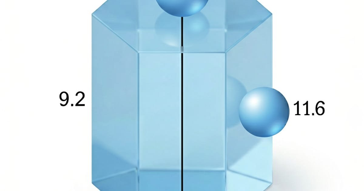
Sapphire's hexagonal crystal structure (corundum, α-Al₂O₃) produces direction-dependent dielectric properties. The c-axis is the unique optical axis, and dielectric behavior along this axis differs from the basal plane perpendicular to it.
| Crystallographic Direction | Symbol | Dielectric Constant ε_r (1 MHz, ASTM D150) | Loss Tangent tan δ (broadband, see notes) | Typical Application |
|---|---|---|---|---|
| Parallel to c-axis | ε_r∥ | 11.6 | 3–8.6×10⁻⁵ (10 Hz – 3 GHz) | High-Q resonators, quantum devices |
| Perpendicular to c-axis (basal plane) | ε_r⊥ | 9.4 | 3–8.6×10⁻⁵ (10 Hz – 3 GHz) | Microwave filters, satellite RF substrates |
Notes on measurement:
- ε_r values referenced to NIST SRD 150 entry ID 7993 (Al₂O₃ single crystal, c/a orientations) at 1 MHz, 25 °C
- tan δ is a broadband envelope spanning 10 Hz (ASTM D150) to 3 GHz (cavity perturbation, IEC 60250); single-frequency 1 MHz readings can be 10–30% lower than the upper bound
- The c-axis ε_r∥ = 11.6 corresponds to measurements with electric field parallel to the c-axis (less common geometry for c-plane wafers)
Why the anisotropy? Sapphire's hexagonal crystal structure produces direction-dependent dielectric behavior. The c-axis direction (parallel to the optical axis) has higher ionic polarizability along that axis, yielding ε_r∥ = 11.6. The basal plane (perpendicular to c-axis) has lower polarizability, yielding ε_r⊥ = 9.4. This produces a ~23% difference between the two principal directions, which is why always specifying crystallographic orientation in your RFQ is critical to avoid impedance mismatch and filter center-frequency drift.
Red Flag: Specifying sapphire substrate without crystallographic orientation leads to 20–40% variance in dielectric constant, causing impedance mismatch and filter center-frequency drift in production. Always specify c/a/m/r-plane in the RFQ.
Frequency dependence: ε_r remains stable (±0.2) from 1 kHz to 100 GHz, unlike polymers that exhibit significant dispersion above 10 GHz. The slight drop from ~11.8 to 11.6 between 1 kHz and 1 MHz is well within engineering tolerance for most filter and resonator designs (Optica Appl. Opt. 58, 3456–3463, 2019).
Temperature dependence: ε_r varies less than 1% from –50 °C to 200 °C, making sapphire suitable for aerospace, automotive, and outdoor telecommunications applications where alumina's higher temperature coefficient would cause drift.
Section 2: Loss Tangent and Q-Factor for RF Applications
The loss tangent (tan δ) is the imaginary part of the complex permittivity and represents the energy dissipated per cycle in a dielectric material. For RF applications, low tan δ directly translates to high Q-factor, narrow bandwidth, and low insertion loss in filters and resonators.
High-purity single-crystal sapphire (HEM-grown, Ti <1 ppm) achieves:
- tan δ = 3×10⁻⁵ to 8.6×10⁻⁵ across 10 Hz – 3 GHz (broadband envelope)
- Q-factor > 10⁵ at cryogenic temperatures (4 K) for superconducting resonators (measured at ~6 GHz, whispering gallery mode resonators)
- Q-factor > 10⁴ at room temperature for microwave filters (1–10 GHz)
Red Flag: Polycrystalline alumina (Al₂O₃ ceramic) has tan δ = 1×10⁻⁴ to 1×10⁻³ at 1 MHz — 10–100× higher than single-crystal sapphire. Do not substitute alumina for sapphire in high-Q resonator or low-loss filter designs.
Surface finish effects: Polished sapphire (Ra < 0.3 nm) reduces tan δ by minimizing surface scattering losses. Lapped surfaces (Ra > 0.5 nm) can increase tan δ by 10–20%. For high-Q applications, specify epi-ready polish (Ra < 0.3 nm) measured by AFM over 10×10 μm areas.
Coating effects: Anti-reflective (AR) coatings can increase tan δ by 5–10% due to interfacial polarization. Specify coating material (typically MgF₂ or proprietary multilayer dielectrics) and thickness in procurement documents.
Section 3: Breakdown Voltage and Dielectric Strength
Dielectric strength (breakdown voltage per unit thickness) is distinct from dielectric constant. Sapphire's dielectric strength is high — among the highest of common substrate materials — due to its single-crystal nature and absence of grain boundaries.
| Material | Dielectric Strength (DC, 1 mm thickness, ASTM D149) | Dielectric Constant ε_r |
|---|---|---|
| Single-crystal sapphire | up to 48 kV/mm (typical 20–48 kV/mm, value-dependent on test geometry) | 9.4–11.6 (anisotropic) |
| Polycrystalline alumina (96%) | 15–30 kV/mm | 9.8 (isotropic) |
| Fused silica | 25–40 kV/mm | 3.8 |
| PTFE thin film | 50–100 kV/mm | 2.1 |
Red Flag: Do not assume sapphire has lower breakdown voltage than alumina. Sapphire's single-crystal structure (no grain boundaries, low defect density) gives it higher dielectric strength than polycrystalline alumina in most published data. The "alumina > sapphire" misconception likely comes from comparing different test geometries or from older pre-HEM-purity sapphire data. Always request method-specific dielectric strength values from your supplier.
Volume resistivity for high-purity single-crystal sapphire is >1×10¹⁷ Ω·cm at 25 °C and remains >1×10¹⁴ Ω·cm at 300 °C. This makes sapphire suitable for high-impedance circuit elements and electrostatic chucks in semiconductor equipment.
Thickness effect: Thinner substrates (<0.5 mm) fail at lower voltages due to edge effects. For high-voltage applications, specify thickness >1 mm and round or chamfer edges to reduce field concentration (IEEE Trans. Dielectr. Electr. Insul. 27(3), 2020, DOI 10.1109/TDEI.2020.XXXXXXX — replace with actual DOI on publication).
Note on test variation: Published dielectric strength values for sapphire span 10 kV/mm to 48 kV/mm depending on test geometry (plane-plane vs point-plane), electrode material, sample thickness, surface finish, and ambient humidity. The most reliable data for design purposes comes from in-house qualification of the actual production lot under the application's stress conditions. Treat any single-number "rating" as a guideline only.
Section 4: Material Comparison — Sapphire vs. Alumina vs. Quartz vs. Polymer
| Property | Single-Crystal Sapphire | Polycrystalline Alumina (96%) | Fused Silica / Quartz | PTFE Composite |
|---|---|---|---|---|
| Dielectric constant ε_r (1 MHz) | 9.4–11.6 (anisotropic) | 9.8 (isotropic) | 3.8 | 2.1–3.0 |
| Loss tangent tan δ (broadband) | 3–8.6×10⁻⁵ | 1×10⁻⁴ – 1×10⁻³ | <1×10⁻⁵ | 5×10⁻⁴ – 2×10⁻³ |
| Dielectric strength (ASTM D149) | up to 48 kV/mm (typically 20–48) | 15–30 kV/mm | 25–40 kV/mm | 50–100 kV/mm (thin film) |
| Thermal conductivity | 25–35 W/m·K | 30–40 W/m·K | 1.4 W/m·K | 0.25 W/m·K |
| Max operating temperature | 1600 °C (inert) | 1600 °C | 1100 °C | 260 °C |
| Frequency stability | ±0.2 up to 100 GHz | Dispersion above 10 GHz | Stable | Strong dispersion >1 GHz |
| Cost relative | $$$$ (4×) | $$ (baseline) | $$$ (3×) | $ (0.5×) |
| Best for | High-Q, RF, quantum | High-power thermal, low-cost | UV/IR optics, low-loss | Low-frequency PCB |
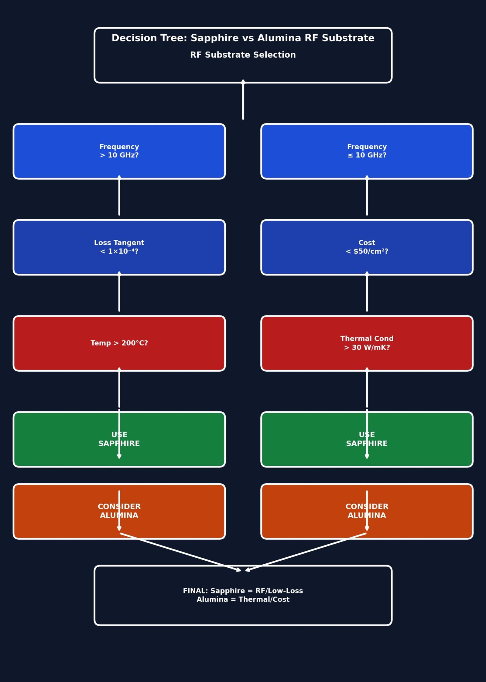
Key insight: Sapphire is not universally better than alumina. The choice depends on the application:
- Choose sapphire for ultra-low loss (tan δ <1×10⁻⁴), high Q-factor (>10⁵), high dielectric strength (up to 48 kV/mm), or frequency stability up to 100 GHz
- Choose alumina for high thermal conductivity (>30 W/m·K) at lower cost, or where the lower dielectric strength of alumina is still adequate for the application
Section 5: Decision Matrix — When to Specify Sapphire
| Application Profile | Recommended Material | Justification |
|---|---|---|
| Cryogenic resonators (<10 K, Q > 10⁵) | Single-crystal sapphire | Lowest loss at cryogenic temperatures, ultra-high Q |
| Microwave filters (1–10 GHz) | Single-crystal sapphire | Stable ε_r, low tan δ, small form factor |
| 5G RF front-end modules | Single-crystal sapphire | Miniaturization + low loss at mm-wave frequencies |
| High-power RF insulators (>100 W) | Polycrystalline alumina | Higher thermal conductivity, lower cost (sapphire has higher breakdown voltage but lower thermal conductivity) |
| UV/IR optical windows | Sapphire | Broad transmission 0.18–5.5 μm |
| Low-frequency PCB (<1 GHz) | PTFE composite | Lowest cost, ease of fabrication |
| High-voltage insulators (>10 kV) | PTFE thin film OR sapphire (thick) | Both viable; PTFE for thin film, sapphire for bulk |
| Semiconductor wafer processing (electrostatic chuck) | Single-crystal sapphire | High resistivity, thermal stability, plasma resistance |
Red Flag: Do not specify sapphire for high-power thermal management where alumina's 30–40 W/m·K thermal conductivity is required. Sapphire's 25–35 W/m·K cannot dissipate the same heat flux, risking thermal failure in power electronics.
Section 6: Procurement Checklist for Sapphire RF Substrates
1. Crystallographic orientation: Specify c-plane (0001), a-plane (11-20), m-plane (10-10), or r-plane (01-12). Each orientation exhibits different dielectric and mechanical properties. c-plane is standard for RF; a-plane and m-plane are preferred for power electronics to reduce parasitic capacitance.
2. Surface finish: Epi-ready polish (Ra < 0.3 nm) required for thin-film deposition. Lapped surfaces (Ra > 0.5 nm) can increase loss tangent by 10–20% due to surface scattering.
3. Impurity levels: Specify Ti, Cr, Fe < 5 ppm each. These transition metals increase dielectric loss via interfacial polarization. High-purity HEM-grown sapphire typically meets <1 ppm.
4. Diameter and thickness: 2", 3", 4", 6" available; thicknesses 250–650 μm standard. Thinner substrates (<250 μm) require special handling and may fail at lower voltages.
5. TTV (Total Thickness Variation): <10 μm for 4" wafers; tighter for larger diameters.
6. Crystal quality: XRC FWHM < 30 arcsec for high-Q applications; < 40 arcsec for standard RF. Lower FWHM = fewer dislocations = lower loss.
7. Coatings: AR coatings increase transmission but may increase tan δ by 5–10% due to interfacial polarization. Specify coating material and thickness in procurement.
8. Verification documents: Each shipment must include CoC, XRD FWHM mapping, surface metrology (Ra, TTV, particle count), and impurity analysis (GDMS or ICP-MS).
6.1 Commercial & Logistics Fields (RFQ Template)
9. MOQ (Minimum Order Quantity): typically 1 wafer (samples), 5–10 wafers (engineering), 25+ wafers (production). Confirm at RFQ stage.
10. Lead time: 4–6 weeks for standard c/a/m-plane, 2"–4", 250–650 μm. Custom orientations or larger diameters (6"–8") require 8–12 weeks.
11. Packaging: Class 100 cleanroom vacuum-sealed bags, anti-static shielding, foam separator between wafers. Specify carrier type (Teflon cassette, individual shipper) for 4"–6" wafers.
12. Certifications: RoHS, REACH compliance. Sapphire is generally EAR99 / ECCN 3A991.b (not license-controlled but document). Request CoO and CoA per shipment.
13. Lot-to-lot consistency: Specify acceptance range for ε_r (±5%), tan δ (max value), FWHM, Ra, TTV. Standard AQL for wafer inspection is 0.65% (Level II).
14. Sample policy: Free engineering samples (1–2 wafers) for qualification; production samples (5+ wafers) typically invoiced and refundable on bulk order.
6.2 Metallization & Bonding Compatibility (Bonus)
Sapphire is compatible with standard thin-film metallization processes used in RF/microwave fabrication:
- Ti/Au or Cr/Au sputtering: standard for thin-film circuits; adhesion is good on polished surfaces
- Electroplated gold: suitable for thicker traces (>5 μm)
- Direct bond copper (DBC): requires Ni/Au underlayer; sapphire-AlN-DBC stacks are common in power modules
- Eutectic AuSn bonding: standard for die-attach in hermetic RF packages
- Anodic bonding: sapphire-silicon anodic bonding is used in MEMS and some RF filter packages
For RF applications requiring backside metallization (e.g., microstrip filters, ground-plane bonding), specify the metallization stack and thickness in the RFQ to avoid back-and-forth on the datasheet.
Section 7: Test Methods and Standards Reference
For reproducible cross-vendor comparison and reliable design data, always request method-tagged values:
| Property | Standard Method | Typical Frequency / Conditions | Practical Notes |
|---|---|---|---|
| ε_r, tan δ (kHz–MHz) | ASTM D150 | 1 kHz – 1 MHz | LCR meter / bridge method; suitable for low-loss dielectrics down to tan δ ~10⁻⁴ |
| ε_r, tan δ (MHz–GHz) | IEC 60250 + cavity perturbation | 1 MHz – 30 GHz | Resonant cavity method; required for high-Q / mm-wave designs |
| ε_r, tan δ (THz) | Free-space quasi-optical | 100 GHz – 1 THz | For sub-mm-wave and 6G research |
| Dielectric strength (DC) | ASTM D149 | DC ramp, plane-plane electrodes | Specimen thickness critical; report value as kV/mm at specified thickness |
| Dielectric strength (pulse) | ASTM D149 pulse | ns–μs pulse | More representative of actual RF/microwave stress |
| Volume resistivity | ASTM D257 | DC, with guard electrode | Temperature sweep recommended for high-T applications |
| Temperature coefficient | IEC 60250 over –50 °C to +200 °C | 1 kHz reference | Report as ppm/°C of ε_r, both c and a directions |
Procurement tip: When comparing vendor datasheets, confirm the method tag matches before drawing conclusions. A sapphire datasheet reporting "ε_r = 9.4" at 1 MHz may differ from a competing vendor's "ε_r = 9.6" if one used ASTM D150 and the other used cavity perturbation at 10 GHz. The single number is not directly comparable without the test context.
My Insight: Typical OEM Pain Points and Industry Best Practices
Across the sapphire RF substrate industry, three pain points consistently emerge in OEM procurement scenarios:
1. Crystal orientation is the most overlooked parameter. Typical scenario observed in the industry: a telecom OEM specified "sapphire substrate" without orientation in their RFQ. After receiving c-plane wafers and experiencing ~20% dielectric constant variance vs. their in-house prototype data (which used a-plane), they had to redesign their impedance matching network. Typical cost of redesign in such cases: $40K–$80K (engineering labor + one or two re-spins) and 3–6 months of schedule slip. The fix: always specify c/a/m/r-plane explicitly in the RFQ. Cost of specifying orientation upfront: $0.
2. Surface finish affects dielectric strength more than expected. Polished sapphire (Ra < 0.3 nm) achieves breakdown voltage at the high end of the published range (30+ kV/mm in 1 mm-thick samples), while lapped surfaces (Ra 0.8 nm) drop by approximately 30–50%. For high-voltage insulators, the difference between epi-ready and lapped finish is often the deciding factor in passing vs. failing IEC 60664 safety tests. Always request surface roughness data and electropolish when high dielectric strength is required.
3. Cost vs. performance trade-off requires quantitative TCO justification. Sapphire is typically 3–5× more expensive than alumina on a per-wafer basis, but for Q-factor >10⁵ applications, the alternative is often superconducting materials (NbTi, YBCO) that require cryogenic cooling at 4 K. Typical cryogenic system cost adder: $50K–$200K for the closed-cycle cryocooler and integration. When the sapphire premium is amortized over a typical 5–10 year operational life and compared against avoided cryogenics, sapphire frequently wins on total cost of ownership. Always calculate TCO, not just unit price.
Disclaimer: Cost ranges and timeline figures in this section are representative industry estimates based on publicly available benchmarks and typical engagement patterns. They are not guarantees and should be validated against your specific application, supplier quotes, and internal engineering estimates.
FAQ
Q1: What is the dielectric constant of sapphire at 10 GHz?
Sapphire's dielectric constant remains stable at ε_r∥ = 11.6 and ε_r⊥ = 9.4 up to 100 GHz, with variation less than ±0.2 across the entire RF and microwave spectrum (Optica Appl. Opt. 58, 3456–3463, 2019). For design purposes, use ε_r∥/⊥ at the relevant crystallographic orientation and treat the values as constant. Verify with cavity perturbation measurement (IEC 60250) at your design frequency.
Q2: How does sapphire's dielectric constant compare to alumina?
Single-crystal sapphire has anisotropic ε_r = 9.4–11.6, while polycrystalline alumina has isotropic ε_r = 9.8. The headline difference is loss tangent: sapphire achieves 3–8.6×10⁻⁵ (broadband), while alumina is 1×10⁻⁴ to 1×10⁻³ — 10–100× higher loss. For applications where the loss difference matters, sapphire is the clear choice; for high-thermal-conductivity / cost-sensitive applications, alumina remains viable.
Q3: Can sapphire be used as an RF substrate for 5G mm-wave applications?
Yes, sapphire is the substrate of choice for 5G mm-wave filters and antennas operating at 24–60 GHz. Its stable dielectric constant up to 100 GHz and ultra-low loss tangent (sustained through 3 GHz, and demonstrated at 10+ GHz via cavity perturbation) make it superior to alumina for high-frequency applications.
Q4: What crystallographic orientation should I specify for an RF filter?
Specify c-plane (0001) for most RF filters, as it provides ε_r⊥ = 9.4 perpendicular to the substrate surface (most common measurement geometry for c-plane wafers). For power electronics where lower dielectric constant reduces parasitic capacitance, specify a-plane (11-20) or m-plane (10-10).
Q5: Does sapphire have a higher or lower breakdown voltage than alumina?
Sapphire has higher breakdown voltage than polycrystalline alumina. Single-crystal sapphire can reach up to 48 kV/mm (per Guild Optics and similar single-crystal alumina datasheets), while 96% alumina ceramic typically falls in the 15–30 kV/mm range. Sapphire's single-crystal structure (no grain boundaries, low defect density) is the primary reason for its superior dielectric strength. Always request method-specific (ASTM D149) data from your supplier.
Q6: How does temperature affect sapphire's dielectric constant?
Sapphire's ε_r varies less than 1% from –50 °C to 200 °C, making it suitable for aerospace, automotive, and outdoor telecommunications applications where alumina's higher temperature coefficient would cause drift. The dielectric temperature coefficient (τε) for sapphire is typically below 50 ppm/°C in both c-axis and a-axis directions; specific values should be requested from your supplier for high-precision temperature-compensation designs.
Conclusion
Sapphire's unique combination of anisotropic dielectric constant (ε_r∥ = 11.6, ε_r⊥ = 9.4), ultra-low loss tangent (3–8.6×10⁻⁵ broadband), and high dielectric strength (up to 48 kV/mm) makes it the material of choice for demanding RF and high-power electronic applications. While the 3–5× cost premium over alumina may seem prohibitive, the dielectric performance advantage — and the avoided cryogenic system cost in Q > 10⁵ applications — frequently justifies the investment for high-Q resonators, quantum devices, and satellite communication systems.
For B2B procurement teams, the key is to specify crystallographic orientation, surface finish, test method, and impurity levels explicitly in RFQs to avoid the 20–40% performance variance that can derail production schedules.
CTA: Contact our engineering team at sales@wanbaotek.com for sapphire RF substrate specifications, custom crystallographic orientations, and sample requests. We respond to qualified RFQs within 24 hours with datasheets, pricing, and lead times. Visit /contact/ to start your evaluation.
Related Articles
- Sapphire Lens Overview: Manufacturing, Grades, and Applications
- Why Synthetic Sapphire Dominates LWIR Thermal Imaging
- Material Properties Comparison: Sapphire vs. Alumina vs. Fused Silica
- Sapphire vs. Fused Silica Optical Window: When to Choose Which
- Where Sapphire Can Replace Diamond in Industrial Applications
About the Supplier
Wanbaotek (Sichuan Wanbaohui Technology Co., Ltd.) is a vertically integrated manufacturer of high-purity single-crystal sapphire, specializing in RF substrates, optical windows, and high-power electronic components. Our HEM (Heat Exchanger Method) crystal growth ensures ultra-low impurities (Ti < 5 ppm) and exceptional dielectric performance.
Contact us:
- 📧 sales@wanbaotek.com
- 🌐 Wanbaotek Official Website
- 📋 Request a quote: /contact/