
Sapphire Wafer Cleaning: A Comprehensive Buyer's Guide
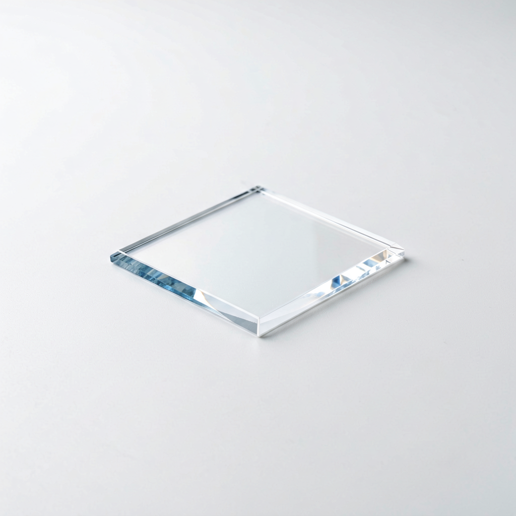
Sapphire wafer cleaning removes surface contaminants from Al2O3 substrates to meet optical and semiconductor specifications. This guide explains cleaning methods, contamination sources, and selection criteria for procurement engineers. Sapphire (Al2O3) has Mohs hardness of 9, transmission from 0.18 to 5.5 μm, and is used in demanding optical and electronic applications. Proper cleaning is essential for coating adhesion, epitaxial growth, and device reliability. For more background, see our industrial sapphire window overview.
Why Sapphire Wafer Cleaning Matters
Sapphire wafers serve as substrates for LEDs, RFICs, and optical components. Surface contamination can cause epitaxial defects, coating delamination, or optical scatter. Even sub-micron particles can degrade performance. Cleaning removes organic residues, metallic ions, particles, and native oxide layers. The goal is a chemically clean, particle-free surface without damaging the substrate.
| Contaminant Type | Example | Risk |
|---|---|---|
| Organic | Oils, photoresist | Poor adhesion, haze |
| Metallic | Fe, Cu, Na | Electrical degradation |
| Particulate | Dust, polishing debris | Scratches, scatter |
| Native oxide | Al2O3 layer | Epitaxial defects |
Common Cleaning Methods
Solvent Cleaning
Solvent cleaning uses acetone, isopropanol, or proprietary blends to dissolve organic contaminants. Typical process: ultrasonic bath in acetone, then isopropanol, followed by deionized (DI) water rinse. This is often the first step. It does not remove metallic ions or particles effectively.
Acid Cleaning
Acid solutions remove metallic contaminants and native oxide. A common mixture is sulfuric acid and hydrogen peroxide (piranha), or hydrochloric acid and nitric acid (aqua regia). These are aggressive and require proper safety equipment. Acid cleaning can etch the surface if not controlled.
Alkaline Cleaning
Alkaline solutions, such as ammonium hydroxide and hydrogen peroxide (RCA SC-1), remove particles and organics. They also create a thin chemical oxide that can be removed with dilute HF. Alkaline cleaning is common in semiconductor processing.
Plasma Cleaning
Plasma cleaning uses reactive gases (O2, Ar) to remove organics and activate the surface. It is dry, fast, and leaves no chemical residues. Plasma cleaning is effective for surfaces that cannot tolerate wet chemicals. It is often used before coating or bonding.
UV-Ozone Cleaning
UV-ozone cleaning oxidizes organic contaminants using UV light and ozone. It is gentle and suitable for delicate surfaces. It does not remove particles or metals.
Brush Scrubbing
Brush scrubbing mechanically removes particles using a soft brush and DI water. It is effective for large particles but may scratch soft surfaces. Sapphire is hard (Mohs 9), so scratching is unlikely.
Comparison of Cleaning Methods
| Method | Contaminants | Pros | Cons |
|---|---|---|---|
| Solvent | Organics | Simple, safe | Poor for particles/metals |
| Acid | Metals, oxide | Effective | Hazardous, can etch |
| Alkaline | Particles, organics | Standard in semi | Leaves oxide |
| Plasma | Organics | Dry, no residue | Needs vacuum |
| UV-ozone | Organics | Gentle | Slow |
| Brush | Particles | Mechanical | Not for sub-micron |
Selecting a Cleaning Process
Choosing a cleaning process depends on the wafer's end use, contamination level, and surface sensitivity. For optical coatings, a clean surface is critical for adhesion. For epitaxial growth, metallic contamination must be below 1e10 atoms/cm2. For demanding applications, a combination of methods is often used.
Consider these factors:
- End use: optical, electronic, or biological
- Contamination type and level
- Surface roughness requirements
- Chemical compatibility
- Process cost and throughput
Based on typical OEM procurement data, a standard cleaning sequence is: solvent clean, acid clean, DI water rinse, and dry. For ultra-clean surfaces, add plasma or UV-ozone.
Incoming Inspection and Handling
Sapphire wafers from suppliers may have residual polishing slurry or packaging residues. Perform incoming inspection: visual check, particle count, and contact angle measurement. Store wafers in clean, sealed containers to avoid contamination. Handle with clean gloves or tweezers to prevent fingerprints.
Cleanroom and Quality Control
Cleaning should be performed in a cleanroom environment to avoid recontamination. Class 100 or better is recommended for critical applications. Quality control methods include:
- Particle count using laser surface scanner
- Contact angle measurement for organic cleanliness
- XPS or SIMS for metallic contamination
- AFM for surface roughness
According to SEMI standards, particle counts and metallic contamination levels have specific limits. Ensure your supplier follows these standards.
Common Mistakes in Sapphire Wafer Cleaning
- Using low-purity chemicals that leave residues
- Inadequate rinsing leading to chemical spots
- Drying with air that contains oil or particles
- Touching the surface with bare hands
- Skipping incoming inspection
Avoid these mistakes to ensure consistent results.
Advanced Cleaning Considerations
Chemical Purity and Grade
For sapphire wafer cleaning, the purity of chemicals is critical. Semiconductor-grade (SEMI) or electronic-grade chemicals have lower trace metal content, typically below parts per billion. Using lower-grade solvents can introduce metallic contaminants, defeating the purpose of cleaning. Always specify the grade in your procurement requirements.
Water Quality
Deionized (DI) water used for rinsing must have high resistivity, typically 18.2 MΩ·cm, to avoid leaving ionic residues. Ultrafiltration may be needed to remove particles from the water. The rinse water quality directly affects final cleanliness.
Drying Methods
After wet cleaning, drying is essential to prevent water spots. Common methods include spin drying, hot nitrogen blow-off, and IPA vapor drying. Spin drying is fast and effective for flat wafers. Hot nitrogen blow-off is gentle but may not remove all water from complex geometries. IPA vapor drying leaves no residue and is preferred for critical applications. The choice depends on wafer size and throughput.
Process Integration
In a production environment, cleaning is often integrated with other steps. For example, in LED manufacturing, sapphire wafers are cleaned before epitaxial growth. The cleaning process must be compatible with the subsequent process. For instance, if the wafer will undergo high-temperature processing, any residual organics can cause carbon contamination. Therefore, a final oxygen plasma clean may be required.
Environmental and Safety Considerations
Wet cleaning involves hazardous chemicals. Proper ventilation, personal protective equipment (PPE), and waste disposal are mandatory. Acid and solvent waste must be neutralized or treated before disposal. Plasma cleaning uses gases that may require special handling. Always follow local regulations and supplier safety data sheets.
Application-Specific Cleaning Protocols
LED Substrates
For LED epitaxy, sapphire wafers must be free of metallic ions and particles. A typical protocol: solvent clean (acetone/IPA), RCA SC-1, dilute HF dip, DI rinse, and spin dry. The final surface should have a contact angle below 10 degrees.
Optical Components
For optical windows and lenses, cleaning focuses on removing organic residues and particles that cause scatter. A gentle protocol: UV-ozone or plasma clean, followed by DI rinse. Avoid aggressive acids that can etch the surface and increase roughness.
Semiconductor Devices
For RFICs and other semiconductor devices, metallic contamination must be minimized. A rigorous protocol: piranha clean, RCA SC-1 and SC-2, dilute HF, and megasonic rinse. This sequence removes organics, particles, and metals.
Medical and Biological Applications
Sapphire is used in some medical devices due to its biocompatibility. Cleaning must ensure no toxic residues. Use biocompatible cleaning agents and validate the process. Sterilization may be required, but it can affect surface properties.
Procurement Checklist for Cleaning Services
When outsourcing sapphire wafer cleaning, consider the following:
- Certifications: ISO 9001, ISO 14001
- Cleanroom class and monitoring
- Chemical purity and water quality
- Process validation and documentation
- Incoming and outgoing inspection reports
- Packaging and shipping methods
- Lead time and capacity
- Cost per wafer and minimum order quantity
Ask for a certificate of conformance (CoC) and test data for each batch.
FAQ
What is the best method for sapphire wafer cleaning?
The best method depends on the contamination and end use; a combination of solvent and acid cleaning is common.
Can I use ultrasound for sapphire wafer cleaning?
Yes, ultrasonic agitation improves cleaning efficiency, but frequency and power must be controlled.
Does cleaning damage the sapphire surface?
Properly controlled cleaning does not damage sapphire, but aggressive acids can etch if overexposed.
How do I measure cleaning effectiveness?
Contact angle measurement and particle count are standard methods.
How often should I clean sapphire wafers?
Clean immediately before use or coating; storage time should be minimized.
Do you offer cleaning services for sapphire wafers?
We provide custom cleaning as part of our precision component services; contact us for details.
What purity chemicals are required?
Use semiconductor-grade or electronic-grade chemicals to avoid residues.
How do I store cleaned sapphire wafers?
Store in a clean, sealed container with desiccant to minimize contamination.
What is the typical turnaround time for cleaning services?
Standard cleaning services typically have a 3-5 business day turnaround, depending on volume and specifications. For large orders, we can schedule production to meet your timeline.
Can you clean patterned sapphire substrates (PSS)?
Yes, we have experience cleaning PSS for LED applications. The process is adjusted to avoid damaging the patterned surface.
Do you provide cleaning validation reports?
Yes, we can provide particle count, contact angle, and other test data upon request.
About Wanbaotek (Sichuan Wanbaohui Technology Co., Ltd.)
Wanbaotek supplies high-quality sapphire windows, lenses, and precision substrates. We provide custom components for optical, semiconductor, and scientific applications. For inquiries, email sales@wanbaotek.com. Learn more about our sapphire precision components or how we make sapphire windows. Request a quote for your sapphire wafer cleaning needs by contacting us.